Ocs package: Difference between revisions
Jump to navigation
Jump to search
| Line 286: | Line 286: | ||
V1 Va 0 SIN(0.5 0.5 1 0 0) | V1 Va 0 SIN(0.5 0.5 1 0 0) | ||
V2 Vb 0 SIN(0.5 0.5 2 0.25 0) | V2 Vb 0 SIN(0.5 0.5 2 0.25 0) | ||
V3 Vdd 0 1 | V3 Vdd 0 1 | ||
.END | .END | ||
Revision as of 06:33, 22 September 2015
OCS : Octave Circuit Simulator
History and Motivation
Problem Formulation
Data Structure
File Formats
Tutorials
A CMOS AND GATE
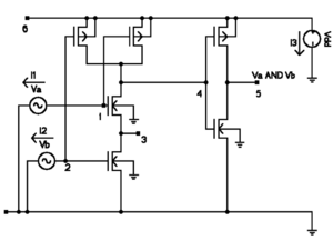
Here we show how to set up the simulation of the CMOS AND gate in the figure. The circuit has
- 9 Elements
- 6 MOSFETs (3 n-type + 3 p-type)
- 3 Voltage sources
Below we show three methods for constructing the circuit data structure
Once the circuit data structure is loaded the simulation can be started by the following commands
| Code: Run the AND gate simulation |
x         = [.5 .5 .33 .66 .5 1 0 0 1 ]';
t         = linspace (0, .5, 100);
pltvars   = {"Va", "Vb", "Va_and_b"};
dmp       = .2;
tol       = 1e-15;
maxit     = 100;
out       = tst_backward_euler (outstruct, x, t, tol, maxit, pltvars);
|
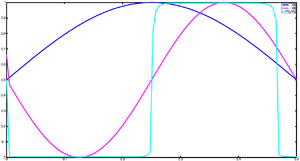
Click on the figure to the right to see the simulation results
Build the AND GATE structure directly
| Code: Build the AND GATE structure via an Octave script |
## NLC

# n-type
outstruct.NLC(1).func = "Mnmosfet";
outstruct.NLC(1).section = "simple";
outstruct.NLC(1).nextvar = 4;
outstruct.NLC(1).npar = 3;
outstruct.NLC(1).nparnames = 3;
outstruct.NLC(1).parnames = { "k", "Vth", "rd"};

outstruct.NLC(1).pvmatrix = [1.0000e-04   1.0000e-01   1.0000e+07
                             1.0000e-04   1.0000e-01   1.0000e+07
                             1.0000e-04   1.0000e-01   1.0000e+07];

outstruct.NLC(1).vnmatrix = [1   3   4   0
                             2   0   3   0
                             4   0   5   0];

outstruct.NLC(1).nintvar = [0 0 0];
outstruct.NLC(1).osintvar = [0 0 0];


# p-type
outstruct.NLC(2).func = "Mpmosfet";
outstruct.NLC(2).section = "simple";
outstruct.NLC(2).nextvar = 4;
outstruct.NLC(2).npar = 3;
outstruct.NLC(2).nparnames = 3;
outstruct.NLC(2).parnames = { "k", "Vth", "rd"};
outstruct.NLC(2).pvmatrix = [-1.0000e-04  -1.0000e-01   1.0000e+07
                             -1.0000e-04  -1.0000e-01   1.0000e+07
                             -1.0000e-04  -1.0000e-01   1.0000e+07];
outstruct.NLC(2).vnmatrix =  [ 1   6   4   6
                               2   6   4   6
                               4   6   5   6];

outstruct.NLC(2).nintvar = [0 0 0];
outstruct.NLC(2).osintvar = [0 0 0];

# Va and Vb

outstruct.NLC(3).func = "Mvoltagesources";
outstruct.NLC(3).section = "sinwave";
outstruct.NLC(3).nextvar = 2;
outstruct.NLC(3).npar = 4;
outstruct.NLC(3).nparnames = 4;
outstruct.NLC(3).parnames = {"Ampl", "f", "delay", "shift"};
outstruct.NLC(3).pvmatrix = [0.50000   1.00000   0.00000   0.50000
                             0.50000   2.00000   0.25000   0.50000];
outstruct.NLC(3).vnmatrix = [ 1   0
                              2   0];
outstruct.NLC(3).nintvar = [1 1];
outstruct.NLC(3).osintvar = [0 0];

## LCR

# Vdd
outstruct.LCR(1).func = "Mvoltagesources";
outstruct.LCR(1).section = "DC";
outstruct.LCR(1).nextvar = 2;
outstruct.LCR(1).npar = 1;
outstruct.LCR(1).nparnames = 1;
outstruct.LCR(1).parnames = {"V"};
outstruct.LCR(1).pvmatrix = 1;
outstruct.LCR(1).vnmatrix = [6 0];
outstruct.LCR(1).nintvar = 1;
outstruct.LCR(1).osintvar = 2;

##

outstruct.namesn = [1   2   5   6   7   8   9];
outstruct.namess = {"Va", "Vb", "Va_and_b", "Vdd", "I1", "I2", "I3"};
outstruct.totextvar =  6;
outstruct.totintvar =  3;
|
Build the AND gate circuit structure parsing an IFF netlist
| Code: Load the AND circuit structure parsing an IFF netlist |
outstruct = prs_iff ("and");
|
| Code: IFF netlist for the AND gate (.cir file) |
% 0.1b1
% A Simple CMOS AND GATE
%
% N-Mosfets
% There are 3 N-Mosfets
Mnmosfet simple 4 3
3 3
k          Vth		rd
1e-4       0.1		1e7
1e-4       0.1		1e7
1e-4       0.1		1e7
1 3 4 0
2 0 3 0
4 0 5 0
%
% P-Mosfets
Mpmosfet simple 4 3
3 3
k           Vth		rd
-1e-4       -0.1	1e7
-1e-4       -0.1	1e7
-1e-4       -0.1	1e7
1 6 4 6
2 6 4 6
4 6 5 6
%
% Input voltage sources
Mvoltagesources sinwave 2 4
2 4
Ampl      f       delay     shift
0.5       1       0.0       0.5
0.5       2       0.25      0.5
1 0
2 0
END
%
% Power supply
Mvoltagesources DC  2 1
1 1
V
1
6 0
END
|
| Code: IFF netlist for the AND gate (.nms file) |
% 0.1b1
1 Va
2 Vb
5 Va_and_b
6 Vdd
7 I1
8 I2
9 I3
|
| Code: Model evaluator file for simple MOSFET models |
function [a,b,c] = Mnmosfet (string, parameters, parameternames, extvar, intvar, t)

  switch string

    case 'simple',

      rd = 1e6;

      for ii=1:length(parameternames)
        eval([parameternames{ii} "=",...
              num2str(parameters(ii)) " ;"])
      endfor

      vg   = extvar(1);
      vs   = extvar(2);
      vd   = extvar(3);
      vb   = extvar(4);

      vgs  = vg-vs;
      vds  = vd-vs;

      if (vgs < Vth)


        gm = 0;
        gd = 1/rd;
        id = vds*gd;

      elseif ((vgs-Vth)>=(vds))&(vds>=0)

        id = k*((vgs-Vth)*vds-(vds^2)/2)+vds/rd;
        gm = k*vds;
        gd = k*(vgs-Vth-vds)+1/rd;

      elseif ((vgs-Vth)>=(vds))&(vds<0)

        gm = 0;
        gd = 1/rd;
        id = vds*gd;

      else # (i.e. if 0 <= vgs-vth <= vds)

        id = k*(vgs-Vth)^2/2+vds/rd;
        gm = k*(vgs-Vth);
        gd = 1/rd;

      endif

      a = zeros(4);

      b = [ 0     0         0   0;
           -gm   (gm+gd)   -gd  0;
            gm  -(gm+gd)    gd  0;
            0     0         0   0];

      c = [0 -id id 0]';
      break;

    otherwise

      error(["Mnmosfet: unknown option " string]);

  endswitch

endfunction
|
Build the AND gate circuit structure parsing a .spc file
| Code: Load the AND circuit structure parsing a .spc file |
outstruct = prs_spice ("and");
|
| Code: The .spc file for the CMOS AND gate |
* AND (simple Algebraic MOS-FET model)

.MODEL mynmos NMOS(LEVEL=simple k=2.94e-05   Vth=0.08	rd=.957e7)
.MODEL mypmos PMOS( k=-2.94e-05   Vth=-0.08	rd=.957e7)

M1 Va 3  4        0 mynmos
M2 Vb 0  3        0 mynmos
* nside of the inverter
M3 4  0  Va_and_b 0 mynmos

M4 Va Vdd 4        Vdd  mypmos
M5 Vb Vdd 4        Vdd  mypmos

* pside of the inverter
M6 4  Vdd Va_and_b Vdd  mypmos

V1  Va 0 SIN(0.5 0.5 1 0 0)
V2  Vb 0 SIN(0.5 0.5 2 0.25 0)
V3  Vdd 0 1

.END
|

