Ocs package: Difference between revisions
Jump to navigation
Jump to search
| Line 17: | Line 17: | ||
** 3 Voltage sources | ** 3 Voltage sources | ||
For the MOSFETs we use a very simple algebraic model defined by the following code | For the n-type MOSFETs we use a very simple algebraic model defined by the following code | ||
{{Code|Model evaluator file for simple MOSFET models |<syntaxhighlight lang="octave" style="font-size:13px"> | {{Code|Model evaluator file for simple MOSFET models |<syntaxhighlight lang="octave" style="font-size:13px"> | ||
Revision as of 06:38, 22 September 2015
OCS : Octave Circuit Simulator
History and Motivation
Problem Formulation
Data Structure
File Formats
Tutorials
A CMOS AND GATE
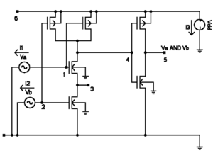
Here we show how to set up the simulation of the CMOS AND gate in the figure. The circuit has
- 9 Elements
- 6 MOSFETs (3 n-type + 3 p-type)
- 3 Voltage sources
For the n-type MOSFETs we use a very simple algebraic model defined by the following code
| Code: Model evaluator file for simple MOSFET models |
function [a,b,c] = Mnmosfet (string, parameters, parameternames, extvar, intvar, t)

  switch string

    case 'simple',

      rd = 1e6;

      for ii=1:length(parameternames)
        eval([parameternames{ii} "=",...
              num2str(parameters(ii)) " ;"])
      endfor

      vg   = extvar(1);
      vs   = extvar(2);
      vd   = extvar(3);
      vb   = extvar(4);

      vgs  = vg-vs;
      vds  = vd-vs;

      if (vgs < Vth)


        gm = 0;
        gd = 1/rd;
        id = vds*gd;

      elseif ((vgs-Vth)>=(vds))&(vds>=0)

        id = k*((vgs-Vth)*vds-(vds^2)/2)+vds/rd;
        gm = k*vds;
        gd = k*(vgs-Vth-vds)+1/rd;

      elseif ((vgs-Vth)>=(vds))&(vds<0)

        gm = 0;
        gd = 1/rd;
        id = vds*gd;

      else # (i.e. if 0 <= vgs-vth <= vds)

        id = k*(vgs-Vth)^2/2+vds/rd;
        gm = k*(vgs-Vth);
        gd = 1/rd;

      endif

      a = zeros(4);

      b = [ 0     0         0   0;
           -gm   (gm+gd)   -gd  0;
            gm  -(gm+gd)    gd  0;
            0     0         0   0];

      c = [0 -id id 0]';
      break;

    otherwise

      error(["Mnmosfet: unknown option " string]);

  endswitch

endfunction
|
The model for the p-type devices is entirely analogous.
Below we show three methods for constructing the circuit data structure
Once the circuit data structure is loaded the simulation can be started by the following commands
| Code: Run the AND gate simulation |
x         = [.5 .5 .33 .66 .5 1 0 0 1 ]';
t         = linspace (0, .5, 100);
pltvars   = {"Va", "Vb", "Va_and_b"};
dmp       = .2;
tol       = 1e-15;
maxit     = 100;
out       = tst_backward_euler (outstruct, x, t, tol, maxit, pltvars);
|
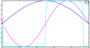
Click on the figure to the right to see the simulation results
Build the AND GATE structure directly
| Code: Build the AND GATE structure via an Octave script |
## NLC

# n-type
outstruct.NLC(1).func = "Mnmosfet";
outstruct.NLC(1).section = "simple";
outstruct.NLC(1).nextvar = 4;
outstruct.NLC(1).npar = 3;
outstruct.NLC(1).nparnames = 3;
outstruct.NLC(1).parnames = { "k", "Vth", "rd"};

outstruct.NLC(1).pvmatrix = [1.0000e-04   1.0000e-01   1.0000e+07
                             1.0000e-04   1.0000e-01   1.0000e+07
                             1.0000e-04   1.0000e-01   1.0000e+07];

outstruct.NLC(1).vnmatrix = [1   3   4   0
                             2   0   3   0
                             4   0   5   0];

outstruct.NLC(1).nintvar = [0 0 0];
outstruct.NLC(1).osintvar = [0 0 0];


# p-type
outstruct.NLC(2).func = "Mpmosfet";
outstruct.NLC(2).section = "simple";
outstruct.NLC(2).nextvar = 4;
outstruct.NLC(2).npar = 3;
outstruct.NLC(2).nparnames = 3;
outstruct.NLC(2).parnames = { "k", "Vth", "rd"};
outstruct.NLC(2).pvmatrix = [-1.0000e-04  -1.0000e-01   1.0000e+07
                             -1.0000e-04  -1.0000e-01   1.0000e+07
                             -1.0000e-04  -1.0000e-01   1.0000e+07];
outstruct.NLC(2).vnmatrix =  [ 1   6   4   6
                               2   6   4   6
                               4   6   5   6];

outstruct.NLC(2).nintvar = [0 0 0];
outstruct.NLC(2).osintvar = [0 0 0];

# Va and Vb

outstruct.NLC(3).func = "Mvoltagesources";
outstruct.NLC(3).section = "sinwave";
outstruct.NLC(3).nextvar = 2;
outstruct.NLC(3).npar = 4;
outstruct.NLC(3).nparnames = 4;
outstruct.NLC(3).parnames = {"Ampl", "f", "delay", "shift"};
outstruct.NLC(3).pvmatrix = [0.50000   1.00000   0.00000   0.50000
                             0.50000   2.00000   0.25000   0.50000];
outstruct.NLC(3).vnmatrix = [ 1   0
                              2   0];
outstruct.NLC(3).nintvar = [1 1];
outstruct.NLC(3).osintvar = [0 0];

## LCR

# Vdd
outstruct.LCR(1).func = "Mvoltagesources";
outstruct.LCR(1).section = "DC";
outstruct.LCR(1).nextvar = 2;
outstruct.LCR(1).npar = 1;
outstruct.LCR(1).nparnames = 1;
outstruct.LCR(1).parnames = {"V"};
outstruct.LCR(1).pvmatrix = 1;
outstruct.LCR(1).vnmatrix = [6 0];
outstruct.LCR(1).nintvar = 1;
outstruct.LCR(1).osintvar = 2;

##

outstruct.namesn = [1   2   5   6   7   8   9];
outstruct.namess = {"Va", "Vb", "Va_and_b", "Vdd", "I1", "I2", "I3"};
outstruct.totextvar =  6;
outstruct.totintvar =  3;
|
Build the AND gate circuit structure parsing an IFF netlist
To parse an IFF format netlist of the CMOS AND gate we can use the following command
| Code: Load the AND circuit structure parsing an IFF netlist |
outstruct = prs_iff ("and");
|
The IFF netlist consists of the .cir file named "and.cir" shown below
| Code: IFF netlist for the AND gate (.cir file) |
% 0.1b1
% A Simple CMOS AND GATE
%
% N-Mosfets
% There are 3 N-Mosfets
Mnmosfet simple 4 3
3 3
k          Vth		rd
1e-4       0.1		1e7
1e-4       0.1		1e7
1e-4       0.1		1e7
1 3 4 0
2 0 3 0
4 0 5 0
%
% P-Mosfets
Mpmosfet simple 4 3
3 3
k           Vth		rd
-1e-4       -0.1	1e7
-1e-4       -0.1	1e7
-1e-4       -0.1	1e7
1 6 4 6
2 6 4 6
4 6 5 6
%
% Input voltage sources
Mvoltagesources sinwave 2 4
2 4
Ampl      f       delay     shift
0.5       1       0.0       0.5
0.5       2       0.25      0.5
1 0
2 0
END
%
% Power supply
Mvoltagesources DC  2 1
1 1
V
1
6 0
END
|
and of the .nms file named "and.nms shown below
| Code: IFF netlist for the AND gate (.nms file) |
% 0.1b1
1 Va
2 Vb
5 Va_and_b
6 Vdd
7 I1
8 I2
9 I3
|
Build the AND gate circuit structure parsing a .spc file
| Code: Load the AND circuit structure parsing a .spc file |
outstruct = prs_spice ("and");
|
| Code: The .spc file for the CMOS AND gate |
* AND (simple Algebraic MOS-FET model)

.MODEL mynmos NMOS(LEVEL=simple k=2.94e-05   Vth=0.08	rd=.957e7)
.MODEL mypmos PMOS( k=-2.94e-05   Vth=-0.08	rd=.957e7)

M1 Va 3  4        0 mynmos
M2 Vb 0  3        0 mynmos
* nside of the inverter
M3 4  0  Va_and_b 0 mynmos

M4 Va Vdd 4        Vdd  mypmos
M5 Vb Vdd 4        Vdd  mypmos

* pside of the inverter
M6 4  Vdd Va_and_b Vdd  mypmos

V1  Va 0 SIN(0.5 0.5 1 0 0)
V2  Vb 0 SIN(0.5 0.5 2 0.25 0)
V3  Vdd 0 1

.END
|

